

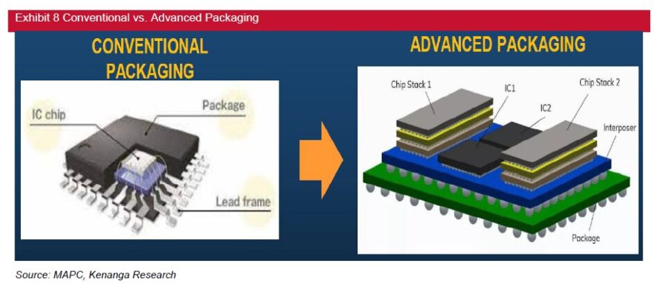
ADVANCED PACKAGING has emerged as a critical pathway to extend semiconductor performance scaling as traditional Moore’s Law becomes increasingly constrained.
While chip performance has historically been driven by transistor shrinking and migration to more advanced process nodes, this approach is becoming more challenging due to EUV limitations, rising process complexity, higher design costs and weaker economics at leading-edge nodes.
As a result, the industry is shifting from pure transistor-level scaling towards system-level (or integrated circuit) scaling.
Rather than relying on one large monolithic chip, chipmakers are increasingly integrating multiple specialised dies within a single package.
Advanced packaging is becoming increasingly important because traditional chip packaging is no longer enough to meet the performance, power efficiency and miniaturisation requirements of modern electronics.
The main purpose of advanced packaging is to place chips closer together, improve data transfer speed, reduce power consumption and allow more functions to be integrated into smaller devices.
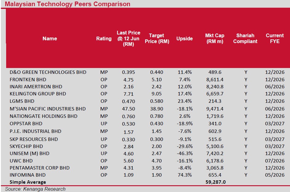
Malaysia stands to benefit from the growing adoption of advanced semiconductor packaging, although the opportunities are likely to be concentrated among selected industry players rather than spread across the entire sector.
The country already possesses a well-developed outsourced semiconductor assembly and test (OSAT) ecosystem, providing a solid foundation for future growth.
However, the next phase of value creation will come from higher-end activities such as advanced testing, precision automation, photonics integration, semiconductor process infrastructure and chiplet design support.
Companies with direct exposure to OSAT services, including Inari, MPI and Unisem, are among the most obvious beneficiaries of this trend.
Meanwhile, firms involved in automation and testing solutions could also gain traction as advanced packaging technologies require increasingly sophisticated levels of precision, inspection and process control.
Rather than viewing advanced packaging as a broad catalyst for the entire technology sector, investors should see it as an ecosystem-driven opportunity where the strongest gains are likely to accrue to companies with specialised capabilities and strategic positioning within the semiconductor value chain.
Malaysia had recently forming Malaysia Advanced Packaging Consortium (MAPC) through collaboration among five local companies (namely, Skyechip, FusionAP, Inari, Pentamaster, and NSW Automation) to help upgrade the country’s semicondocutor industry into a higher-value sector.
The government has approved a RM92 mil R&D grant over 24 months for the programme, while industry is conributing RM93 mil, bringing the total to RM185 mil.
From an investment perspective, the initiative is strategically positive but still early-stage. The near-term impact is likely to be capability-building rather than immediate earnings contribution.
However, the read-through is positive for companies with exposure to advanced packaging, ATE, automation, OSAT process development and high-precision engineering.—June 15, 2026
Main image: indiatimes.com